CREOL
Nanophotonics Systems Fabrication Facility
A 3,000 ft2 facility containing Class 100 and Class 1000 clean rooms. Used for the fabrication and study of nanostructured materials and nanophotonic integrated circuits.
The CREOL Nano-Fabrication facility is open to internal and external users. The facility contains a range of nanofabrication tools and related instrumentation, including an electron-beam lithography system (Leica EPBG 5000+), and various etching and deposition tools.
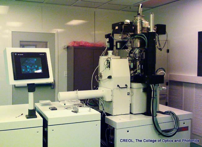
Leica EBPG5000+
Electron beam lithography system is capable of running at 20, 50 and 100 kV, with a minimum spot size of less than 10nm. The main exposure field size may range between 160um X 160um and 1mm X 1mm with a stitching value of less than 50nm. Electron-beam lithography can be performed on a variety of substrate sizes, including five inch masks, three and four inch wafers, and small pieces. A multi-substrate load lock is used to aid in the sequential processing of multiple jobs.
Woollam M2000 Mapping Spectroscopic Ellipsometer (managed by Kik group)
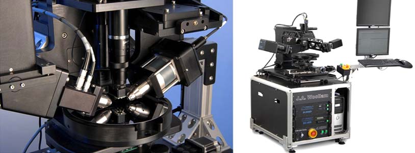
The M2000 High-Speed Scanning Variable Angle Spectroscopic Ellipsometer enables the mapping of layer thickness as well as linear optical properties (refractive index, absorption coefficient, depolarization factors, anisotropy) of single layer or multilayer films at wavelengths between 0.24μm – 1.7μm with a spectral resolution of 3-6nm. The system supports mapping of up to 6” diameter wafers. A complete UV-NIR spectrum can be acquired in 5 seconds with a 0.1 mm spatial resolution.
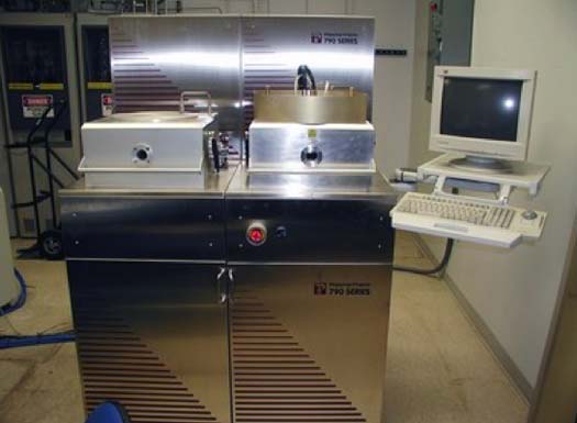
Optoelectronic Fabrication Cleanroom
The 800 sq. ft. cleanroom is a multi-user facility consisting of class 100 and class 10,000 cleanrooms, and is used in the development of optoelectronic semiconductor devices. The facility equipment includes a Suss MJB-3 aligner, a Plasma-Therm 790 RIE/PECVD, an Edwards thermal evaporator, along with a bonder, a scriber and microscope.