Materials Characterization Facility
The Materials Characterization Facility (MCF) is dedicated to providing researchers and industrial partners a place to perform characterization and analysis to advance research; classroom education and hands-on training in the use of state-of-the-art characterization equipment; user-friendly support services with expert advice and data interpretation; and to enhance competitiveness of industrial partners and boost economic development of the Central Florida region.
MCF occupies about 7,000 sq. ft. of space and is supported by 3 full-time research engineers and a full-time facilities coordinator. Collaboration with other Universities is encouraged.
Scanning electron microscopy
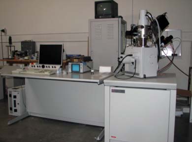
The Zeiss Ultra-55 SEM has a unique design to the final lens; it is electrostatic instead of electromagnetic. This feature allows the microscope to image magnetic materials without distortion from created by a magnetic field. This microscope is also capable of delivering very high lateral resolution at low voltages. The Nabity Electron Beam Lithography system allows researchers to create nanometer scale patterns using the pattern generator in conjunction with the electron beam. The Noran System 7 EDS system with Silicon Drift Detector can acquire the EDS spectrum much faster than a conventional SiLi detector and can detect elements as light as Boron.
- Schottky field emission source
- Resolution 1 nm @ 15 KV, 1.7 nm @ 1 KV
- STEM Detector
- In lens Secondary and Backscatter detectors
- Noran System 7 EDS with Silicon Drift Detector x-ray detector
- Nabity Electron Beam Lithography System

Focused Ion Beam
The 200 TEM FIB removes material by sputtering using gallium at lateral resolution of approximately 5 nm. Platinum metal can also be deposited by ion beam assisted chemical vapor deposition. Gas assisted etching and selective carbon milling may also be performed. FIB has a wide range of applications:
- Specimen preparation for SEM and TEM. TEM cross-section specimens can be prepared within two hours
- Ion channeling contrast imaging
- Device modification – mainly semi-conductor industry