Physics Department
In addition to numerous individual researcher laboratories, the Physics Department has a number of advanced facilities in Shared Facilities labs available for use by all members of the department.
Experimental research facilities within the Department include:
- scanning Raman microscope
- far infrared lasers
- SQUID magnetometry
- x-ray imaging
- photoelectron spectroscopy
- UHV STM/AFM, SIMS, LEED and RHEED
- sputter deposition
- physical vapor deposition
- CVD
- AFM/MFM
- Auger microscopy
- SEM
- EBICS
- many other instruments
Central Florida Nanofabrication Facility
The Central Florida Nanofabrication Facility is a regional user facility which enables fabrication of state-of-the-art nanoscale electronic, mechanical, spintronic and optoelectronic devices for nanoscale fundamental and applied sciences. The facility is located on the fourth floor of the Physical Sciences building in a purpose-built 2800 square-foot facility containing an ISO class 5 (FED STD class 100) cleanroom. The facility’s capabilities to perform nitride and oxide chemical vapor deposition, deep reactive ion etching, metallization for high throughput lithography processes, and chip packaging are unique to the campus and enhances the other user facilities available on campus. The equipment list is:
- E-beam evaporator
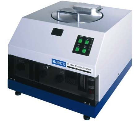
- SAMCO Reactive Ion Etcher (RIE)
- TRION ICP/RIE (MINILock II)
- TRION PECVD (Orion II)
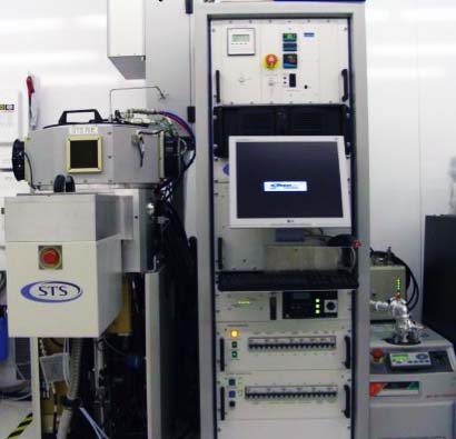
- STS ICP etcher
- Rapid Thermal Annealing / Furnace
- Sputtering system
- OAI Series 200 Mask Aligner
- STS ICP Etcher
- BRANSON/IPC Barrel Etcher
- SPI-DRY™ Critical Point Drier
- Headway PWM32-PS-R790 Spin Coater
- Optical Microscope
- Dektak 3 Profilometer
- Branson B5510 Sonicator
- West Bond 7400C Wire Bonder
- Karl Suss Wafer scriber
- SAMCO Reactive Ion Etcher