Our group explores the extraordinary properties of various emerging nanoscale materials and their translation to transformative technologies through interdisciplinary approaches. A primary focus is on integrating a new class of low-dimensional materials into functional structures and developing a fundamental understanding of their topography-property relationships. A material system of a primary interest at present is two-dimensional (2D) electronic materials wherein every aspect of 2D materials research is explored, including new synthetic methods development, near atomic-scale characterization, and device applications for electronics and energy technologies. Below are some highlights of the past and present researches.
2D materials: Layered transition metal dichalcogenides
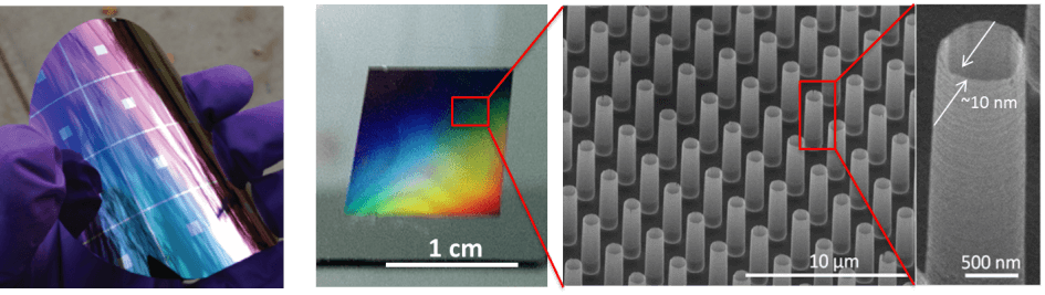
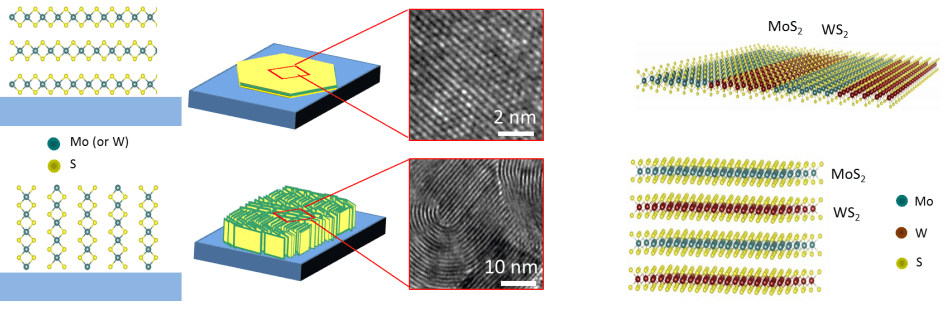
Novel semiconducting 2D materials (e.g., MoS2 or WS2) with controlled morphology and unique chemical heterogeneities are envisioned to present unprecedentedly exciting electrical properties. Current efforts involve the development of novel synthetic methods to realize the large-scale integration of 2D heterostructures and their structural/electrical characterizations.
References
- Metal seed layer thickness-induced transition from vertical-to-horizon growth of MoS2 and WS2 Nano Letters 14, 6842–6849 (2014) [link]
- Chemically synthesized heterostructures of two-dimensional molybdenum/tungsten-based dichalcogenides with vertically aligned layers ACS Nano 8, 95508, (2014) [link]
In-situ transmission electron microscopy (TEM) of dynamic phenomena at nanoscale
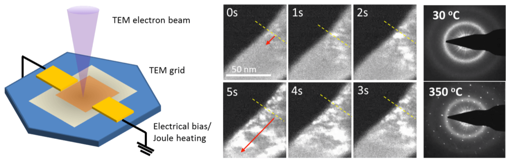
We have pursued to uncover new scientific phenomena uniquely occurring at very small length scales and to understand their fundamental origins. In this endeavor, in-situ TEM techniques that allows for the simultaneous correlation of near atomic structural changes with corresponding physical/electrical properties will be explored.
References
- Nanoscale size effects in crystallization of metallic glass nanorods, Nature Communications, 6, 8157 (2015) [link]
Hybrid nanomaterials for electronics and energy technologies
We are broadly interested in developing novel methodologies to create hybrid nanomaterials with well-defined structures and multi-functionalities for emerging electronics and energy devices.