- Quantum Information Science: Quantum optics based on semiconductor and topological insulator materials, optically mediated quantum information processing with qubits defined in quantum dots that are embedded in nanocavities inside a photonic crystal, quantum cryptography.
- Wide-band Gap Semiconductor Materials: Study nonlinear optical effects, such as 4-wave mixing spectroscopy, many-exciton correlations, single-photon and many-photon entangled-photon sources.
- Topological Insulator and Weyl Semimetal Materials: Study electronic properties of nanostructures linear and nonlinear optical effects, plasmonic effects.
- Graphene: Model mid-IR photodetectors and mid-IR thermal emitters based on the plasmonically enhanced photothermoelectric effect.
- 2D materials beyond graphene: Investigate and model transistors, photodetectors, and sensors based on 2D layered materials. Identify defects suitable for single-photon sources.
- Plasmonics in hybrid metal-semiconductor materials: Model light- and voltage-controlled switches to control the propagation of surface plasmon polaritons.
- Photovoltaics: Develop new nanoparticles for solar energy harvesting, luminescent solar energy concentration for improving current solar panels.
- Water splitting: Develop new nanoparticles for improved photocatalysis.
Acknowledgement of financial support:


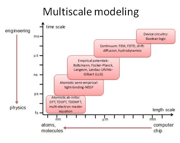
We use multiscale modeling tools (see Figure below) to describe quantum devices for optoelectronics in 2D materials, quantum computing, quantum communication, solar cell concentrators, and ultrasensitive graphene detectors.
A selection of current research topics is given below.
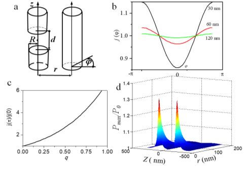
1. Scalable quantum network in a photonic crystal structure:
One of the main challenges of current quantum computing schemes is the scalability to at least 1000 qubits. Our work strives to overcome the problem of scalability and to develop in the future scalable quantum computing architectures that will be able to outperform any classical computer.
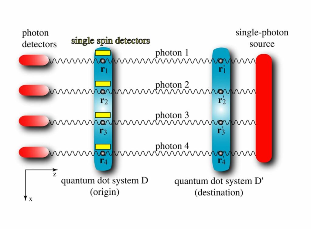
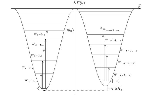
One of our main interests is the description of scalable quantum information processing inside a photonic crystal. We have developed a quantum finite-difference time domain (quantum FDTD) model that describes the propagation of quantum light interacting with quantum dots embedded in nanocavities inside the photonic crystal host. The main goal here is to demonstrate the scalability of this proposed quantum network.
We investigate and quantify the entanglement between electronic spins located in wide-bandgap semiconductor quantum dots embedded inside cavities of the photonic crystal host. The analytical methods include mostly quantum-information scientific models for the calculation of the entanglement and decoherence due to environment (such as phonons, nuclear spins, disorder, etc.) by means of e.g. the von Neumann entropy. The numerical methods include the Finite-Difference Time-Domain (FDTD) technique for electromagnetic waves and standard bandstructure calculations based on tight-binding and pseudopotential methods.
Broader impact: One of the main challenges of current quantum computing schemes is the scalability to at least 1000 qubits, eventually to 1 million qubits. Our work strives to overcome the problem of scalability and to develop in the future scalable quantum computing architectures that will be able to outperform any classical computer.
For details, see the following publication:
- Gabriel Gonzalez, Hubert Seigneur, Winston V. Schoenfeld, Michael N. Leuenberger, Invited Review Article: Theory of a Scalable Electron-Spin based Quantum Network inside a Photonic Crystal, Journal of Computational and Theoretical Nanoscience, Special Issue on “Technology Trends and Theory of Nanoscale Devices for Quantum Applications”, 7, 1651-1672 (2010).
- Michael N. Leuenberger, Fault-tolerant quantum computing with spins using the conditional Faraday rotation, Phys. Rev. B 73, 075312 (2006).
- Michael N. Leuenberger, Michael E. Flatte, D. D. Awschalom, Teleportation of electronic many-qubit states via single photons, Phys. Rev. Lett. 94, 107401 (2005).
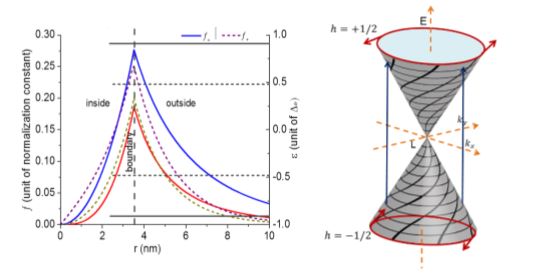
2. Optically mediated quantum information processing and quantum memory with 3D topological insulator quantum dots:
Topological insulators have attracted a lot of interest because of the protection of electron conductance against backscattering process, which relies on Kramer’s pair degeneracy. We investigated theoretically the spectroscopic selection rules for these Kramer’s pair states. These selection rules provide the possibility to read and write quantum information optically, thereby implementing quantum memory. We demonstrate that 3D topological insulator quantum dots can be used to implement optically mediated quantum information processing.
Broader impact: Since the conductance of electrons and holes is topologically protected from backscattering, low-voltage microchips could be developed based on topological insulators. This means that future electronic devices based on topological insulators will consume much less energy, which will especially benefit the mobile electronic devices, such as laptops and mobile cell phones. Besides these obvious benefits, the absence of backscattering could increase the decoherence time for quantum memory, which could enable future quantum computing architectures based on topological insulators.
For details, see the following publication:
- Hari P. Paudel, Michael N. Leuenberger, Three-dimensional topological insulator quantum dot for optically controlled quantum memory and quantum computing, Phys. Rev. B 88, 085316 (2013).
3. High-temperature single-photon source:
We investigate decoherence-assisted tunnelling phenomena in semiconductor heterostructures and quantum-optical effects of the single-photon emission inside a cavity. The numerical methods include finite difference techniques.
For details, see the following publication:
- Sergio Tafur, Michael N. Leuenberger, Spontaneous Creation of Photonic States in Quantum Dots, Reviews in Nanoscience and Nanotechnology 1, 152 (2012).
- Sergio Tafur, Michael N. Leuenberger, Computational Model of Single-Photon Near-Field Emission, Proceedings SPIE 8057, 805704 (2011).
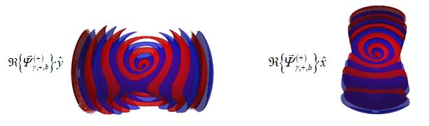
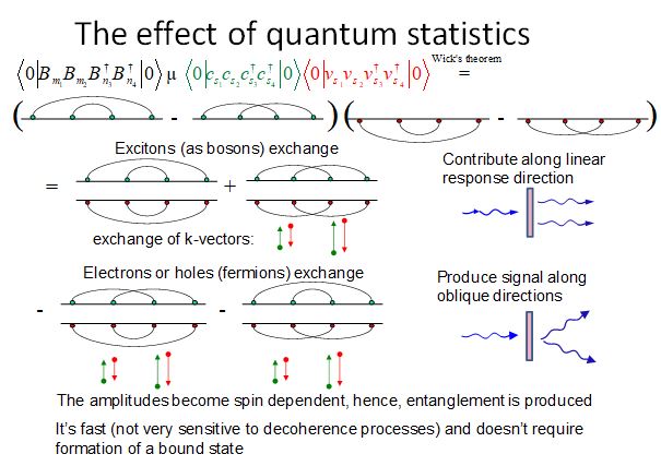
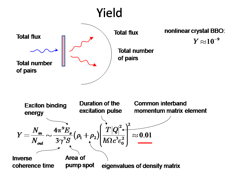
4. Entangled photon source:
We take advantage of many-body correlations and entanglement among excitons in quantum dots and quantum wells to create highly entangled many-photon states, such as GHZ and N00N states. It has been shown that N00N states can be used in the field of quantum metrology to enhance the resolution of imaging and lithography by a factor corresponding to the number of entangled photons. Our recent results demonstrate the possibility to entangle 60 photons inside a cavity, which will lead to a 60-fold enhanced spatial resolution for imaging devices, while keeping the wavelength unchanged.
Broader impact: Our results demonstrate that it is possible to produce highly entangled many-photon states, which can be used for quantum metrology. Our proposed theoretical methods based on the interaction of 60 photons with a few semiconductor quantum dots inside a cavity demonstrate the possibility to entangle 60 photons, which is a breakthrough compared to the currently experimentally achievable 8-photon entanglement based on parametric down-conversion in nonlinear crystals, such as beta-barium borate or lithium niobate.
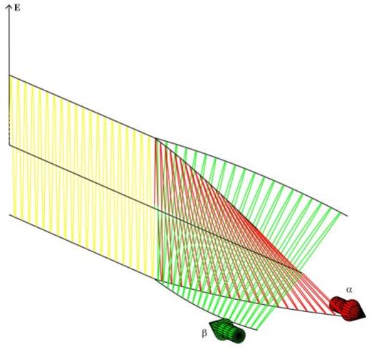
The many-body quantum correlations among excitons leads to an ultraefficient creation of entangled photons:
For details, see the following publication:
- Mikhail Erementchouk, Michael N. Leuenberger, Entanglement of photons due to nonlinear response of quantum wells, Phys. Rev. B 81, 195308 (2010).
5. Quantum computing with single-molecule magnets:
Shor and Grover demonstrated that a quantum computer can outperform any classical computer in factoring numbers and in searching a database by exploiting the parallelism of quantum mechanics. Whereas Shor’s algorithm requires both superposition and entanglement of a many-particle system, the superposition of single-particle quantum states is sufficient for Grover’s algorithm. Here we propose an implementation of Grover’s algorithm that uses molecular magnets, which are solid-state systems with a large spin; their spin eigenstates make them natural candidates for single-particle systems.
Broader impact: We show theoretically that molecular magnets can be used to build dense and efficient memory devices based on the Grover algorithm. In particular, one single crystal can serve as a storage unit of a dynamic random access memory device. Fast electron spin resonance pulses can be used to decode and read out stored numbers of up to 105, with access times as short as 1010 seconds. We show that our proposal should be feasible using the molecular magnets Fe8 and Mn12.
For details, see the following publication:
- Michael N. Leuenberger and Daniel Loss, Quantum Computing in Molecular Magnets, Nature 410, 789-793 (2001).
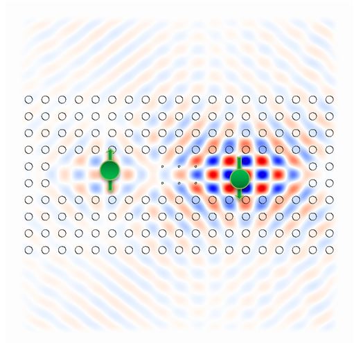
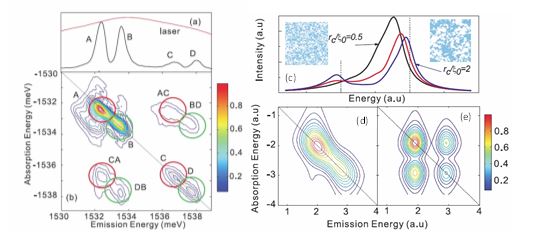
We investigate the photon statistics and 2D 4-wave mixing resulting from Anderson localization of excitons in quantum wells. We are studying the dependence of statistics of photons (with special emphasis on entanglement and antibunching) emitted in the course of radiative decay of classically excited excitons on the global spatial structure of the exciton states in disordered quantum wells. We expect to see antibunching behavior and significant changes in entanglement properties as we reach the regime of Anderson localization. We are currently expanding the notion of the geometric quantization used for analysis of the optics of semiconductor excitations under strong confinement potential to the case when the quantization is supported by the structure of the states.
For details, see the following publication:
- Yuri D. Glinka, Zheng Sun, Mikhail Erementchouk, Michael N. Leuenberger, Alan D. Bristow, Steven T. Cundiff, Allan S. Bracker, Xiaoqin Li, Coherent coupling between exciton resonances governed by the disorder potential, Phys. Rev. B 88, 075316 (2013).
- Yuri D. Glinka, Zheng Sun, Mikhail Erementchouk, Chandriker K. Dass, Michael N. Leuenberger, Allan S. Bracker, Xiaoqin Li, Non-local coherent coupling between excitons in a disordered quantum well, New J. Phys. 15, 075026 (2013).
- Mikhail Erementchouk, Michael N. Leuenberger, Nonlinear Optics in Semiconductor Nanostructures (featured on cover page), book chapter, Handbook of Nanophysics: Nanoelectronics and Nanophotonics, pages 29-1 to 29-20, Edited by Klaus D. Sattler (Taylor-Francis, 2010).
- Mikhail Erementchouk, Michael N. Leuenberger, Lu J. Sham, Non-perturbative phenomena in semiconductor four-wave mixing spectra, Phys. Rev. B 79, 085307 (2009).
- Mikhail Erementchouk, Michael N. Leuenberger, Lu J. Sham, Many-body interaction in semiconductors probed with 2D Fourier spectroscopy, Phys. Rev. B 76, 115307 (2007).
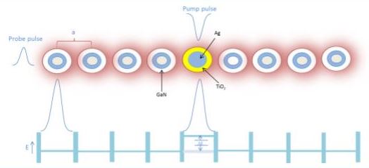
We developed a light-controlled switch for the propagation of surface plasmon polaritons along a chain of nanoparticles made of Ag/TiO2 and Ag/GaN.
Broader impact: Controlling the propagation of surface plasmon polaritons is one of the key requirements for the implementation of plasmonics-based computing, which takes advantage of the reduced effective wavelength of surface plasmon polaritons for decreasing the size of plasmonic transistors. Therefore plasmonics can also be used to miniaturize laser sources and photon detectors and to increase the light-matter interaction.
For details, see the following publication:
- Hari P. Paudel, Michael N. Leuenberger, Light-controlled plasmon switching using hybrid metal-semiconductor nanostructures, Nano Lett. 12, 2690 (2012).
1. Graphene superlattice:
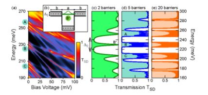
We consider Graphene superlattices for the purpose of identifying Bloch oscillations of Dirac electrons. The goal is to investigate theoretically the negative differential resistance of Graphene superlattices. We found that Graphene superlattices behave very differently from semiconductor superlattices because of the Klein tunneling effect in Graphene. We observe negative differential conductance at voltage biases as low as 10 mV with a high current density, making armchair graphene nanoribbon superlattices attractive for device applications.
Broader impact: A Graphene superlattice can be used to realize negative differential conductance, similar to resonance tunneling diodes. The advantage of Graphene is the high mobility of electrons, which results in less heat dissipation. It is also possible to produce THz radiation, which is crucial for screening of people at airports, satellite-to-satellite communication, outdoor secret short-range communication, indoor wireless communication, medical imaging of skin cancer and tooth erosion, quality assurance of pharmaceuticals, for airline pilots to navigate airplanes through fog, etc.
For details, see the following publication:
- Gerson J. Ferreira, Michael N. Leuenberger, Carlos Egues, Daniel Loss, Low-bias negative differential resistance in graphene nanoribbon superlattices, Phys. Rev. B 84, 125453 (2011).
2. Correlations in an array of self-assembled carbon nanotubes:
Many proposed applications of single walled carbon nanotubes (SWNT) require massively parallel array and selective removal of metallic pathways from the array via electrical breakdown. Since experimental and theoretical studies of individual SWNTs demonstrate that the breakdown is due to joule heating which occurs at random places, a straightforward extrapolation to an array would suggest that the breakdown would occur at random point inside each SWNT. Here we show that in a densely packed aligned array containing up to 30 SWNT/µm, the breakdown of one nanotube leads to a highly correlated breakdown of neighboring nanotubes, thereby producing a nanoscale river shaped pattern. We propose, the origin of correlation is electrostatic field of broken nanotubes that produces locally inhomogeneous current distributions in the neighboring nanotubes triggering their breakdowns. Our results suggest that the densely aligned array works like a correlated solid and have strong implications in the future development of fault-tolerant nano-electronic circuits based on SWNT array.
For details, see the following publication:
- Shashank Shekhar, Mikhail Erementchouk, Michael N. Leuenberger, Saiful I. Khondaker, Correlated breakdown of carbon nanotubes in an ultra-high density aligned array, Appl. Phys. Lett. 98, 243121 (2011).
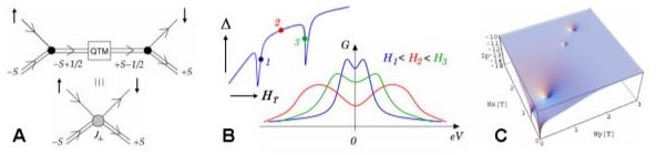
3. Single-electron transistor based on single-molecule magnets:
The goal is to investigate theoretically the physical mechanisms of macroscopic quantum coherence and macroscopic quantum tunneling in quantum transport. We found that it is possible to see topological Berry-phase interference effects in the spin tunneling of molecular magnets which can be detected by means of single-electron tunneling through molecular magnets in a setup similar to a single-electron transistor. The Berry-phase effects are visible in both the Coulomb blockade and spin blockade regime and Kondo regime. The future application includes ultra-small magnetic memory devices. Chemists are working in this direction to create molecular magnets with large anisotropy barriers.
Molecular Magnets can be used for future computer memory chips with ultra-high density. They can also be used to measure ultra-weak magnetic fields. Being able to measure the electronic conductance through single-molecule magnets it will be possible to build magnetic random access memories (MRAM).
For details, see the following publication:
- Gabriel Gonzalez, Michael N. Leuenberger, Eduardo R. Mucciolo, Kondo effect in single-molecule magnet transistors, Phys. Rev. B 78, 054445 (2008).
- Gabriel Gonzalez, Michael N. Leuenberger, Berry-phase blockade in single-molecule magnets, Phys. Rev. Lett. 98, 256804 (2007).
- Michael N. Leuenberger, Eduardo R. Mucciolo, Berry-Phase Oscillations of the Kondo Effect in Single-Molecule Magnets, Phys. Rev. Lett. 97, 126601 (2006).
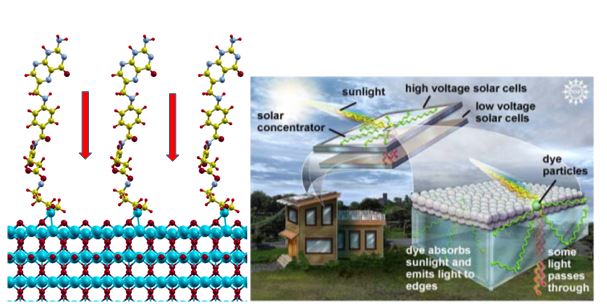
In collaboration with the experimentalist Sudipta Seal here at NSTC, we performed research on TiO2/APTMS/folic acid nanoparticles. The goal is to investigate theoretically the down-conversion of light in hybrid organic-inorganic metal-semiconductor nanoparticles by means of time-dependent density-functional theory (TDDFT) and finite-difference time domain (FDTD) techniques, with main purpose to identify, engineer, and model highly efficient luminescent solar cell concentrators. Recent experiments show an increase in the photocurrent for Si solar cells coated with TiO2/APTMS/folic acid thin film. Recent experiments show also an increase in the efficiency of water splitting using TiO2/APTMS/folic acid thin film.
Broader impact: The world depends strongly on natural gas and oil as an energy resource. However, petroleum is widely used for other more important products, spanning from clothes to medicine. It is therefore vital for the world economy to become more independent by investing efforts into alternative energies, such as solar energy. Our theoretical efforts aim at developing highly efficient solar cells which are cheap, flexible, and mass-producible. Our proposed solar cells are based on hybrid organic-inorganic nanoparticles and polymers, the properties of which can be engineered to maximize the solar harvesting efficiency. Including metallic structures into our nanoparticles provides a means to increase the down-conversion efficiency of nanoparticles by orders of magnitude. This phenomenon relying on plasmonic resonances can be used to build highly efficient luminescent solar energy concentrators.
For details, see the following publication:
- Volodymyr Turkowski, Suresh Babu, Duy Le, Amit Kumar, Manas K. Haldar, Anil V. Wagh, Zongjian Hu, Ajay S. Karakoti, Andre Gesquiere, Benedict Law, Sanku Mallik, Talat S. Rahman, Michael N. Leuenberger, Sudipta Seal, Linker-Induced Anomalous Emission of Organic-Molecule Conjugated Metal-Oxide Nanoparticles, ACS Nano 6, 4854 (2012).
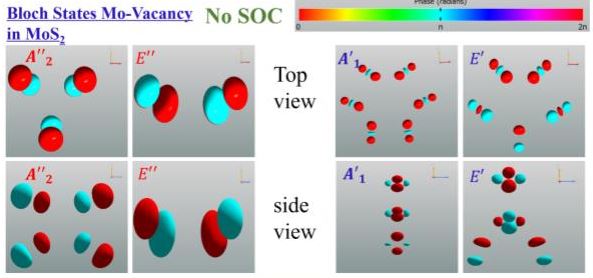
We study different two-dimensional (2D) layered materials and their composites, analyze their structural and physical properties and demonstrate applications in electronics, photonics, and magnetic devices. Novel 2D materials present new opportunities in materials science, physics, chemistry and engineering that are impossible to obtain from their bulk counterpart. For example, molybdenum disulphide (MoS2), a transition metal dichalcogenide (TMDC) is an indirect bandgap semiconductor in the bulk form. However, when it is exfoliated to single layer, it becomes a direct bandgap semiconductor. In addition, the bandgap can be tuned by altering the number of layers of MoS2. Furthermore, since 2D materials are atomically thin, they provide a huge surface area that is open to the environment and can be engineered to obtain desirable properties. The surface of 2D materials can be functionalized with organic ligands, semiconducting molecules, and metal nanoparticles.
Broader impact: 2D materials and composites can have important applications in micro/nano-electronics, optoelectronics, thermoelectric materials, catalysis, hypersensitive sensors, photovoltaics, and energy storage devices.
For details, see the following publication:
- Chandriker K. Dass, M. A. Khan, Genevieve Clark, Je_rey A. Simon, Michael N. Leuenberger,Ricky Gibson, Shin Mou, Xiaodong Xu, Joshua R. Hendrickson, Ultra-Long Lifetimes of Defect Trapped Single Quantum Emitters in Monolayer WSe2/hBN Heterostructures, Adv. Quantum Technol. 2, 1900022 (2019).
- M.A. Khan, Michael N. Leuenberger, Optoelectronics with single layer group-VIB transition metal dichalcogenides, Nanophotonics 7, 1589 (2018).
- M. A. Khan, Michael N. Leuenberger, Room-temperature superparamagnetism due to giant magnetic anisotropy in MoS defected single layer MoS2, J. Phys.: Condens. Matter 30, 155802 (2018).
- M. A. Khan, Mikhail Erementchouk, Joshua Hendrickson, Michael N. Leuenberger, Electronic and Optical Properties of Vacancy Defects in Transition Metal Dichalcogenides, Phys. Rev. B 95, 245435 (2017).
- Mikhail Erementchouk, M. A. Khan, Michael N. Leuenberger, Optical signatures of states bound to vacancy defects in monolayer MoS2, Phys. Rev. B Rapid Communications 92, 075439(R) (2015).
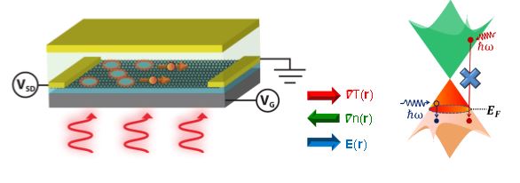
We study nanopatterned graphene not only for increasing the light absorption in the mid-IR regime, but also for ultrafast mid-IR photodetection based on Dirac plasmon-assisted asymmetric hot carrier generation at room temperature. Due to the low photon energy, detection of infrared photons is challenging at room temperature. The photothermoelectric effect offers an alternative mechanism bypassing material bandgap restrictions. In this article, we demonstrate an asymmetric plasmon-induced hot-carrier Seebeck photodetection scheme at room temperature that exhibits a remarkable responsivity of 2900 VW−1, detectivity of 1.1 × 10⁹ Jones along with a fast response of ~100 ns in the technologically relevant 8–12 μm band. This is achieved by engineering the asymmetric electronic environment of the generated hot carriers on chemical vapor deposition grown large area nanopatterned monolayer graphene, which leads to a temperature gradient of 4.7 K across the device terminals for an incident power of 155 nW, thereby enhancing the photothermoelectric voltage by manifold compared to previous reports.
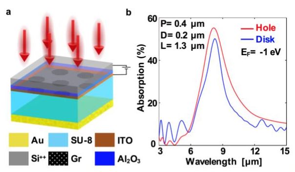
Broader impact: The results presented outline a strategy for uncooled, tunable, and multispectral infrared detection.
For details, see the following publication:
- A. Safaei, S. Chandra, M. W. Shabbir, M. N. Leuenberger, D. Chanda, Nature Communications 10, 3498 (2019).