- Structural Battery
- Dry Processed Batteries
- Cable Supercapacitors
- Plasmonic Structures
- Wearable Energy
- Neuromorphic Synapse
Structural Battery
Safe, long-lasting, and cost-effective energy storage solutions are becoming increasingly vital in today’s society. Zinc and sodium-ion batteries have emerged as promising alternatives to traditional lithium-ion systems, leveraging the abundance and unique properties of their respective charge carriers—zinc and sodium ions. Compared to lithium, both zinc and sodium are significantly more abundant, offering the potential for lower-cost energy storage solutions.
Zinc-ion batteries are well-suited for applications with energy-dense storage requirements due to the large specific capacity of the metallic zinc anode, which is compatible with non-flammable, water-based electrolytes, enhancing both safety and performance. Meanwhile, sodium-ion batteries are renowned for their high cycle life and rapid charge-discharge capabilities, making them ideal for high-power applications, or those requiring frequent and efficient energy turnover. Together, these technologies hold the promise of safer, more affordable, and widely applicable energy storage for a sustainable future.
Dry Processed Batteries
Dry processing of battery electrodes offers several key advantages over traditional slurry-based methods: eliminating solvents shortens processing time, reduces material and energy costs, and enhances cell performance by ensuring uniform binder distribution. Our research focuses on developing a viable dry-processing technique for Zinc-ion battery electrodes.
Cable Supercapacitors
Currently, millions of miles of electrical cables have been used for providing electrical connections in machineries, equipment, buildings and other establishments. Energy storage devices are completely separated from these electrical cables if used. However, it will revolutionize energy storage applications if both electrical conduction and energy storage can be integrated into the same cable. Here, a dual-function coaxial supercapacitor cable (CSC), which has the capability to be used as an electrical cable and an energy storage device, is demonstrated. Similar to typical coaxial cables, the inner core is used for electrical conduction and the overlying layer is used for energy storage. The integrated CSC device shows excellent flexibility and bendability, long and stable cycle lifetimes, and high energy and power densities. All these remarkable results demonstrate a clear technological advance achieved by clubbing electrical conduction and energy storage into one cable.

For details: “Highly Ordered MnO2 Nanopillars for Enhanced Supercapacitor Performance” Adv. Mater. 26, 4279-4285 (2014). (Highlighted by Nature in News & Views).
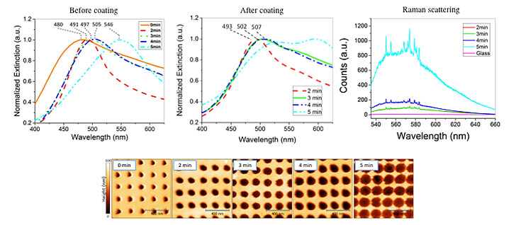
Plasmonic Structures
We have developed a facile fabrication technique for producing tunable plasmonic substrates. With this technique, we are able to tune the plasmon resonance of the substrate to match the molecular resonance of an organic dye with a simple additional fabrication step. Two oscillators can exchange their energies and become coupled when placed in the vicinity of each other. Our nanohole structures are very promising candidate for photon-exciton coupling. This is because nanoscale light confinement is possible with their plasmon resonances. Moreover, since our structures are open cavities, accessing the mode volume in which the coupling take place is relatively easy. This allows us to probe physical/chemical properties of the coupled states. We have found that when we match the plasmon resonance of the nanohole structure to an organic dye such as R6G, Raman scattering signal from the sample is significantly enhanced. Our ongoing research is to explore the use of our fabrication technique to fabricate plasmonic structures with unique properties.
For details:
- Li, J., Madiyar, F., Ghate, S., Kumar, K.S. and Thomas, J., 2023. Plasmonic organic electrochemical transistors for enhanced sensing. Nano Research, 16(2), pp.3201-3206.
- Chantharasupawong, P.; Tetard, L.; Thomas, J., Coupling Enhancement and Giant Rabi-Splitting in Large Arrays of Tunable Plexcitonic Substrates. The Journal of Physical Chemistry C 2014, 118, 23954-23962.
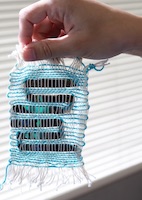
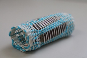
Wearable Energy Storage and Harvesting Ribbons (2016)
Wearable technology has been in the limelight ever since the electronics started becoming smaller and smaller. The miniaturization of gadgets became even easier with the introduction of nanoscience and technology. We have fabricated a flexible and wearable integrated device in the form of thin ribbons which can simultaneously harvest and store energy. An array of such devices are woven into a textile form that can be knitted on clothes. The integrated device consists of a perovskite solar cell on a copper ribbon to harvest the light energy and a thin film supercapacitor on the other side of the ribbon is used to store the charges generated.

Neuromorphic Synapse
The human brain has the power to process and memorize information simultaneously. Neuromorphic computing is designed based on this principle. We recently developed optoelectronic synapsis using a superstructure, which is a baby step in this direction. This superstructure is developed by growing highly photosensitive methylammonium lead bromide perovskite quantum dots (PQDs) on graphene, by a defect-mediated process. Graphene, a two-dimensional sheet of carbon atoms, is a dream material for electronic and optoelectronic applications due to its interesting properties such as broad bandwidths, very high electron mobility and high transparency besides outstanding flexibility and stability. However, a major disadvantage of graphene is the low charge generation efficiency, with only 2.3% of incident light being converted to electric charge. This low charge generation limits its applications in optoelectronic and photonic devices. Contrarily, PQDs have emerged as attractive materials for optoelectronic devices due to their high extinction coefficients, bandgap tunability, high photoluminescence quantum yield, and narrow emission spectrum. However, the charge transport properties of these PQDs are inferior when compared to graphene. By combining these two materials in a superstructure enabled us to achieve high optical absorption and charge transport in an extremely thin medium. The neuromorphic computing ability of our device was tested via face recognition experiments.
Publications:
- Thomas, J., Roy, T., Das, S., Pradhan, B. and Li, J., University of Central Florida Research Foundation Inc UCFRF, 2023. Photonic synapse based on graphene-perovskite quantum dot for neuromorphic computing. U.S. Patent 11,574,177.
- J. Li, P. Dwivedi, K. S. Kumar, T. Roy, K. E. Crawford, J. Thomas, Growing Perovskite Quantum Dots on Carbon Nanotubes for Neuromorphic Optoelectronic Computing. Adv. Electron. Mater. 2021, 7, 2000535. https://doi.org/10.1002/aelm.202000535
- Pradhan, B., Das, S., Li, J., Chowdhury, F., Cherusseri, J., Pandey, D., … & Thomas, J. (2020). Ultrasensitive and ultrathin phototransistors and photonic synapses using perovskite quantum dots grown from graphene lattice. Science advances, 6(7), eaay5225 (2020). DOI:10.1126/sciadv.aay5225