Two-dimensional (2D) semiconductors with near atom thickness present an unusual combination of extremely high mechanical bendability and superior electrical/optical properties, rendering unprecedented opportunities for flexible electronics/optoelectronics. More interestingly, heterogeneously integrating one 2D semiconductor on top of the other achieving vertical stacks of 2D “hetero” structures is envisioned to project even more exciting functionalities impossible with their mono-component counterparts. One of the major hurdles for their technological applications lies in the technical difficulty with precisely integrating them into flexible substrates on a large scale compatible with prevailing microelectronics processes while maintaining their structural integrity.
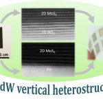
In a recent paper published in Nano Letters, Dr. Yeonwoong (Eric) Jung’s research group reports a viable solution to this problem. By exploring the water-assisted debonding nature of gold interfaced with conventional silicon dioxide growth substrates, they demonstrate the direct growth, transfer, and integration of various 2D hetero-semiconductors on mechanically deformable plastics and metal foils. The size of the integrated 2D hetero-semiconductors reported in this study reaches up to a few centimeter squares, significantly advancing over previous studies which remain to be a few micrometer-scale integrations. By applying this technique, they also demonstrate a new type of 2D/2D vertical heterojunction photo-responsive devices which are difficult to realize with any other conventional approaches.
This study will open a new pathway to explore 2D hetero-semiconductors as novel building-blocks for large-scale emerging electronic/optoelectronic devices of various form factors. Moreover, it will have a significant and broad impact in the field of 2D semiconductors and beyond, accelerating the exploration of unconventional, hierarchically-structured 2D materials and their true technological potential.