As the miniaturization of modern electronic devices continues, scientists have turned to what are now known as two-dimensional (2D) semiconductors which are made up of a few atom thick semiconducting layers – the ultimate size limit of device units.
Some 2D semiconductors such as molybdenum disulfide (MoS2) and tungsten disulfide (WS2) present electrical properties compatible to those of what are already used in the modern electronics industry, but requiring a much lower cost for their preparation. More advantages come from that when these 2D materials bound to each other they create “heterojunctions” which exhibit unusual electrical properties promising for developing new multifunctional electronic devices that have not existed so far. One major hurdle for utilizing these 2D materials has been in how to rationally integrate multiple 2D layers in a scale to be compatible with existing semiconductor manufacturing technologies.
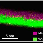
In a recent paper published in Scientific Reports, Jung’s group reports a new chemical synthesis method to stack up multiple 2D semiconductors based on MoS2 and WS2 in a highly controlled manner. These new 2D semiconductors whose thickness was only 7-8 nm were produced on a scale of over a few centimeters square, which is sufficient to cover conventional wafers on which computer chips and light emitting diodes can be integrated. Atomic scale structural characterizations involving electron microscopy directly revealed that two distinct 2D layers perfectly maintained atomically sharp heterojunctions. These novel materials are anticipated to offer tremendous opportunities for emerging technologies across electronics, otpo-electronics and energy areas such as transparent and flexible solar cells that can operate in a muctifunctional manner.