NanoElectronics & NanoPhysics
Diego J. Díaz’s Group deals with electrochemistry and materials chemistry in nanoscale science and technology. In particular, this research focuses on using electrochemistry to create nanostructured surfaces and in the sensing and optoelectronic applications of nanostructured surfaces.
Creation of Nanostructures of Tailored Size and Functionality
The integration of scanning probe microscopies (AFM) and electrochemistry offer the ability to not only image surfaces at very high resolution, but to control interactions on the surface at the nanoscale. We can currently modify an AFM probe with different chemical functionalities, in order to tailor the tip to different chemical reactions. In this technique that we call Redox Probe Microscopy, or tip is the electrochemical probe and it allow us to spatially control the electrochemistry. The careful control of the electrochemistry, together with the high spatial resolution of an AFM allow us to create novel nanolithography patterns on surfaces. After a full chemical, morphology and electrochemical characterization of the modified surface is carried, we can then apply such nanostructured surfaces can then be used for the preparation of devices.
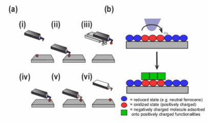
Figure 1. Different schemes for the manipulation of molecular adsorbate with an Redox Probe Microscopy (RPM) tip (a) direct manipulation of adsorbates via the tip interactions. (b) Indirectly, by changing the redox state of an area of an adsorbate, the overall charge can change and allow us to build different structures by changing solutions of different overall charges.
We want to put particular emphasis on magnetic, and electronic properties as this materials can be further studied not only as novel lithography materials (creating desired patterns), but also in areas of charge storage (providing a high density of redox centers), molecular wires, switches or other molecular electronic components, and as novel data storage devices, with the nanometer sized units being able to represent data bits. Molecularly controlled films of metallo-dendrimers and polymers will be used as our modified substrates.
Electronic and Magnetic Properties
The popularity of commercial magneto-optic based storage devices spark a great interest into the preparation and characterization of new magnetic materials for the new generation of magneto-optic devices. For developing a new generation of high density, small size magneto-optical devices, thin films or nanometer scale magnetic domains are required and several tools are accessible to study such films.
The application of the Surface Magneto Optic Kerr Effect or (SMOKE), where the rotation of the polarization plane of light is studied as it is reflected from a magnetized surface combined with Scanning Probe Microscopy (SPM) and its variant known as Magnetic Force Microscopy (MFM) can provide a high spatial resolution characterization of the surface. We are particularly interested in investigating two main situations.
- The study and characterization of magnetized thin films, and magnetized nanostructures based on redox active dendrimers or large ligands, where the magnetization can be modulated electrochemically.
- To gain understanding on the magnetization properties of low dimensionality materials.
Optical and Luminescent Properties of Nanomaterials
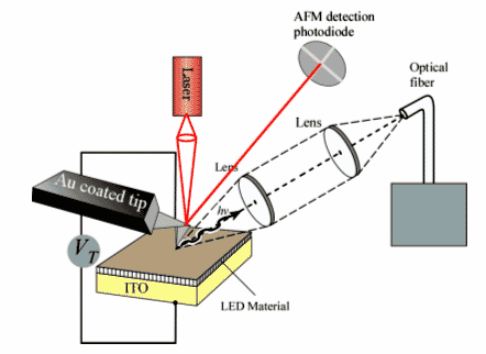
Figure 2. Integrated Atomic Force Microscope – Electroluminescence Miscroscope (AFM-EL) that can be prepared by integrating an optical fiber into an AFM. This will allow us to spatially collect light emission of an LED material using a metal coated AFM tip as the cathode.
Electrochromic refers to the generation of different visible region electronic adsorption bands as a result of switching between different oxidation (redox) states. Many transition metal coordination complexes (polypyridine, phtalocyanides, porphyrins, etc) can be used for these applications. An alternative approach that I propose is the application of dendrimer and ligand films created in a controlled fashion. This might allow me to prepare electrochromic devices of desired dimensions (length or thickness for example) and to combine these materials into more complex topographies, while keeping a good control of the amount of materials.
Moreover, our modified AFM probe can be used as the cathode for the excitation of the LED films, allowing the nanoscale size “turn-on” of areas of the led. We are interested in developing a modified AFM with a fiber-optic detector to be able to detect light emission coming from the localized LED areas. Such approach can be beneficial to the preparation of novel LED materials and optoelectronic devices.
Sensor Device
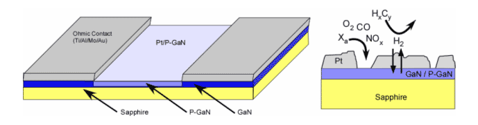
Figure 3. Conductivity based sensor device for the detection of hydrogen gas.
Porous Si (P-Si) has been demonstrated to work as a sensor material of high sensitivity and low detection limits. However, Si and P-Si tend to react to the analyte being detected or to the surrounding environment, affecting device performance and reversibility. GaN has enhanced thermal, chemical and mechanical stability, allowing for reversible, stable and reusable detectors to be prepared. We have developed methodologies that allow us to easily generate porous GaN and other porous materials. As for P-Si, P-GaN based sensors can be based on interferometry, or in conductivity based sensors, where the adsorption of molecules generally induce a change in the conductivity of the semiconductor by providing electronic pathways for current or redistributing charge on the surface. In both cases, the enhanced surface area of the porous semiconductor allows for sub ppm detection and the stability of the P-GaN allows for durable, stable and efficient sensor devices. We are interested in the preparation of novel gas sensors based on the conductivity of GaN based devices and the optimization of such devices.
Such work involves the electrochemical characterization of the P-GaN, the metallization and preparation of the device and the optimization of the performance of the sensor. Such sensors can be used for the detection of Hydrogen and other gases.
For More Information
Dr. Diego J. Díaz
Department of Chemistry
University of Central Florida
Orlando, FL 32816