NanoElectronics & NanoPhysics
My research group is interested in the fabrication of nanoscale electrical and optical devices consisting of low dimensional chemical nanostructures such as nanoparticles, nanowires, nanotubes, and molecules and their electronic transport properties. Nanoscience and nanotechnology deals with the study, development, and application of materials, devices, and systems with dimensions in the 1-100 nm range. The physical, chemical, and biological properties of materials at the nanoscale differ in fundamental and valuable ways from the properties of bulk matter. The many novel phenomena observed at the nanoscale are primarily the consequence of the appearance of quantum effects that begin to play an important role at length scales approaching a few nanometers. Our research effort is directed toward creating and characterizing improved materials, devices, and systems at the nanoscale that exploit these new properties.
Specific areas of research interest includes: (i) Fabrication and quantum transport properties of nanoscale devices using individual nanoparticle and molecule, (ii) Large scale nano-manufacturing of carbon nanotube based electronic devices, and (iii) Organic/inorganic nanocomposites for electronic and photovoltaic devices.
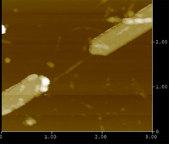
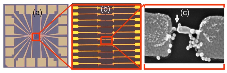
Nanoscale devices using individual nanoparticle and molecule: Fabrication of nanoelectronic devices using single nanoparticle or molecule requires (i) sub 10 nm spaced source and drain electrodes, and (ii) placement of the nanostructures between the nanogap electrodes. We pioneered a technique for the fabrication of sub-10 nm spaced electrodes using current-induced electromigration of a gold nanoparticle metallic bridge. Using these nanospaced electrodes, we fabricated single electron transistors (SET) using metal nanoparticles and measured transport properties of single phenylene-ethynylene molecular junction. Current research effort is directed toward fabricating devices using magnetic nanoparticles and molecules.
Large scale nano-manufacturing of carbon nanotube based electronic devices: Large scale fabrication of controllable and scalable structures using nanowire is of tremendous interest from both technological and fundamental point of view. We are currently developing techniques for the fabrication of such devices using carbon nanotube. Such techniques will enable us to fabricate quantum devices in large scale.
Organic/inorganic nanocomposites for electronic and photovoltaic devices: The organic/inorganic nanocomposite is of tremendous research interest because of its ability to tailor mechanical, optical and electronic properties. By mixing two components, it is possible to design materials that have properties superior to those of individual components. Our current research effort is directed in creating organic/inorganic nanocomposites with tailored electrical, optical and magnetic properties and correlate the nanoscale morphology of the composite with the improved properties.
For More Information
Dr. Saiful Khondaker
NanoScience Technology Center
University of Central Florida
Orlando, FL 32826